
New 3D chip manufacturing technology makes electronics faster and more energy-efficient
TechNews Technology News
June 25, 2025
Author Emma stein
June 25, 2025
Author Emma stein
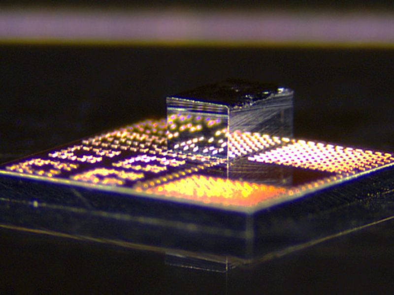
A team from the Massachusetts Institute of Technology has developed a new manufacturing method that can seamlessly integrate high-performance gallium nitride transistors into standard silicon CMOS chips at a lower cost.
Gallium nitride (GaN) is the second most popular semiconductor material after silicon, and is also the key to electronic devices required for the next generation of high-speed communication systems and advanced data centers. In order to achieve higher performance, scientists connect GaN chips to silicon chips, but the welding method limits the size of GaN transistors. If the entire GaN chip is integrated into a silicon chip, the cost is very high, so the road to commercialization is still limited.
To solve this problem, the MIT team recently developed a low-cost, scalable 3D stacking technology that can integrate high-performance GaN transistors into standard silicon CMOS chips and is compatible with existing semiconductor processes, breaking through the existing GaN application limitations, promoting the development of high-speed communications, and is expected to promote cutting-edge technologies such as quantum computing.
The method first builds many tiny transistors on the surface of the GaN chip, then uses fine laser technology to cut each transistor into 240 x 410 microns in size, with a tiny copper pillar on the top of each transistor, and then bonds a certain number of transistors to the silicon chip at -400 ° C, thereby retaining the functions of the two materials and significantly improving performance.
In addition, the GaN circuit is composed of discrete transistors scattered on the silicon chip, which can also reduce the overall system temperature.
The research team used this method to develop a power amplifier and successfully achieved higher signal strength and efficiency than silicon transistor devices. In smartphones, this can improve communication quality, increase wireless bandwidth, enhance connection strength and extend battery life.
This research demonstrates the three-dimensional integration capabilities of multiple gallium nitride chips and silicon CMOS, breaking through the current technological boundaries and is expected to bring faster and more energy-efficient electronic products.
Related links: https://technews.tw/2025/06/25/gallium-nitride-semiconductor-material/
Image source: Massachusetts Institute of Technology
Image source: Massachusetts Institute of Technology
【Disclaimer】
The content of this article only represents the author's personal views and has nothing to do with Creating.
The content, text description and originality have not been verified by this site. This site does not make any guarantee or commitment to this article and all or part of the content, authenticity, completeness, and timeliness. It is for readers' reference only. Please verify the relevant content yourself.
Creating Nano Technologies, Inc.
59 Alley 21 Lane 279, Chung Cheng Road, Yung Kang City, Tainan, TAIWAN
TEL:886-6-2323927 FAX:886-6-2013306 URL: http://www.creating-nanotech.com
59 Alley 21 Lane 279, Chung Cheng Road, Yung Kang City, Tainan, TAIWAN
TEL:886-6-2323927 FAX:886-6-2013306 URL: http://www.creating-nanotech.com