
Creating Nano technology leads packaging innovation with plasma tech, targeting FOPLP and TGV integration.
Economic Daily News
September 10, 2025
By Zhang Jie, Economic Daily
September 10, 2025
By Zhang Jie, Economic Daily
As the global semiconductor industry continues to advance toward higher density, smaller size, and greater computing power, the packaging process has become more than just a terminal step in traditional assembly; it has become a key determinant of chip performance. Taiwan-based Creating Nanotechnology, with years of experience in plasma process equipment, is making a name for itself in next-generation processes such as advanced packaging, panel-level packaging (FOPLP), and through-glass vias (TGV), leveraging its proprietary plasma technology and comprehensive equipment solutions. This is injecting innovative momentum into Taiwan's semiconductor industry.
With over 25 years of experience in the diamond-like carbon (DLC) film field, Creating Nanotechnology once again demonstrated its solid technical foundation and innovative energy. The antistatic composite film technology unveiled at this year's Semiconductor Show is a representative example of its breakthrough in conventional manufacturing. Through a multi-layer PVD/PECVD stacking process, Creating has successfully achieved DLC, not only with its inherent low friction coefficient, wear resistance, and corrosion resistance, but also with antistatic properties, maintaining a stable resistance range of 10^5 to 10^8 Ω. This achievement means that the component can maintain stable electrical properties even in harsh environments ranging from high temperatures of 200°C to low temperatures of -50°C, significantly improving process safety and reliability.

"Currently, power devices, AI chips, and high-performance computing (HPC) chips are increasingly emphasizing system-level packaging and heterogeneous integration. Traditional process methods have long been unable to meet the demands and reliability challenges of sub-micron structures." Creating's nanotechnology team noted that plasma etching and surface activation technologies are now becoming critical to process yield.
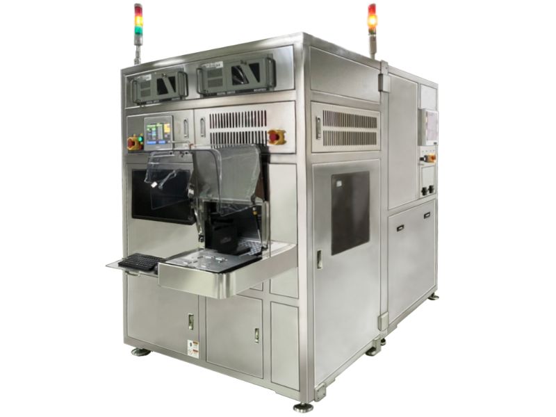
Creating has long invested in the development of high-end tools such as RIE (reactive ion etching), ICP/RIE (inductively coupled plasma), and in-line cleaning equipment, covering not only front-end wafer processing but also flexible back-end packaging needs. In particular, traditional wet processes struggle to achieve high selectivity and low damage in photoresist stripping and PI (polyimide) descum. Creating's plasma systems, through uniform plasma distribution and intelligent parameter control, achieve the dual advantages of rapid cleaning and surface protection.
Facing the extremely high precision requirements of FOPLP (Fan-out Panel Level Packaging) and TGV (Through Glass Via) processes for fine vias and complex structures, Creating's plasma etching technology not only stably controls aspect ratios and sidewall verticality, but also ensures process uniformity and yield improvements. Creating has been successfully implemented in numerous leading advanced packaging manufacturers, becoming an indispensable partner.
Beyond technological advancements, Creating is committed to upgrading its equipment to modularity and intelligence. Through data monitoring, anomaly prediction, and remote control systems, it enhances machine operational stability and production flexibility, effectively reduces labor and consumables costs, and creates long-term competitive advantages for its customers.
"We believe that the future of semiconductors will no longer be solely about chip speed and size, but also about packaging processes. From wafer thinning and photoresist removal to microstructure etching, every step requires millimeter-level precision control, and plasma is a key weapon in this battle." Creating Nano stated that the company is continuously expanding strategic alliances with partners in various fields, including materials, packaging, and testing, and is collaborating with research institutions to introduce AI-powered smart processes, laying a critical foundation for next-generation heterogeneous integration.
Looking ahead, Creating will continue to be driven by innovation, developing more process solutions that meet the needs of AI, high-speed computing, electric vehicles, and 5G applications, and moving towards a complete plasma application ecosystem. As the global chip manufacturing focus shifts to a "packaging-as-process" model, Taiwanese companies with strong technological expertise, like Creating, are crucial drivers in maintaining industry competitiveness and expanding internationally.

Related Link: https://money.udn.com/money/story/5635/8995390
【Disclaimer】
The content of this article only represents the author's personal views and has nothing to do with Creating.
The content, text description and originality have not been verified by this site. This site does not make any guarantee or commitment to this article and all or part of the content, authenticity, completeness, and timeliness. It is for readers' reference only. Please verify the relevant content yourself.
Creating Nano Technologies, Inc.
59 Alley 21 Lane 279, Chung Cheng Road, Yung Kang City, Tainan, TAIWAN
TEL:886-6-2323927 FAX:886-6-2013306 URL: http://www.creating-nanotech.com
59 Alley 21 Lane 279, Chung Cheng Road, Yung Kang City, Tainan, TAIWAN
TEL:886-6-2323927 FAX:886-6-2013306 URL: http://www.creating-nanotech.com