

iPhone 18 Pro Debuts the 2nm A20 Pro: How Does Advanced Packaging Balance AI Performance and Thermal Management?
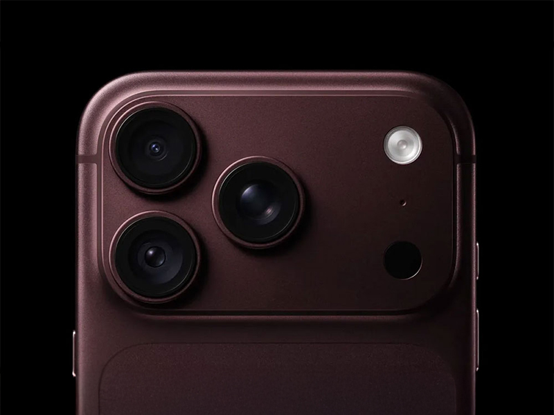
Apple’s next-generation iPhone 18 Pro officially launched on September 18, 2026. Beyond its camera and battery upgrades, the A20 Pro chip—manufactured using a 2nm process—and its redesigned packaging and thermal architecture are particularly noteworthy for the semiconductor industry.
According to Apple, the A20 Pro uses an M-series-inspired packaging design that places the silicon die alongside the memory to improve heat flow and memory bandwidth. Combined with a vapor chamber featuring three times the surface area of the previous generation, Apple claims up to 40% better sustained performance than the iPhone 17 Pro.
Why Does Packaging Matter More as Chips Shrink?
Advanced chips integrate increasingly large numbers of transistors and computing units, while AI workloads place greater demands on memory transfer and heat dissipation.
Even if chip performance improves, thermal resistance, poor interfacial contact or unstable material adhesion within the package may still limit overall performance.
Advanced packaging must therefore address:
- Chip and memory placement and interconnection
- Packaging-material adhesion and thermal conductivity
- Uniformity of metallic films and bonding interfaces
- Control of particles, organic residues and surface oxides
- Thermal-cycle reliability under sustained heavy workloads
How Does Surface Cleanliness Affect Packaging Quality?
High-density packaging contains more microscopic contacts and material interfaces. Before bonding, coating, underfilling or encapsulation, even trace contamination may affect wettability, adhesion, electrical contact and heat transfer.
Plasma cleaning and surface activation can remove organic contamination, modify surface energy and improve subsequent material adhesion. Actual process parameters—including power, treatment time, gas composition and uniformity—must still be optimized according to the substrate, package structure and reliability requirements while minimizing possible surface damage.
Apple has not disclosed the complete A20 Pro manufacturing process, plasma-treatment procedures or suppliers. It would therefore be inappropriate to assume that any specific equipment is involved. However, this example clearly demonstrates that surface cleanliness, film uniformity and interfacial reliability become increasingly important as chips advance toward 2nm nodes and high-density packaging.
Creating Nano Technologies Inc. specializes in atmospheric- and low-pressure-plasma technologies, functional thin films and customized equipment. Surface cleaning, activation and thin-film treatment solutions can be evaluated according to specific material and process requirements.
Sources
- Apple: Official iPhone 18 Pro Product Information
- Reuters: Apple Unveils the iPhone 18 Pro and Its First Foldable iPhone
Creating Nano Technologies, Inc.
59 Alley 21 Lane 279, Chung Cheng Road, Yung Kang City, Tainan, TAIWAN
TEL:886-6-2323927 FAX:886-6-2013306 URL: http://www.creating-nanotech.com