

Are AI Chips Also Vulnerable to Surface Contamination? Plasma Cleaning and Mass-Production Stability in Advanced Packaging
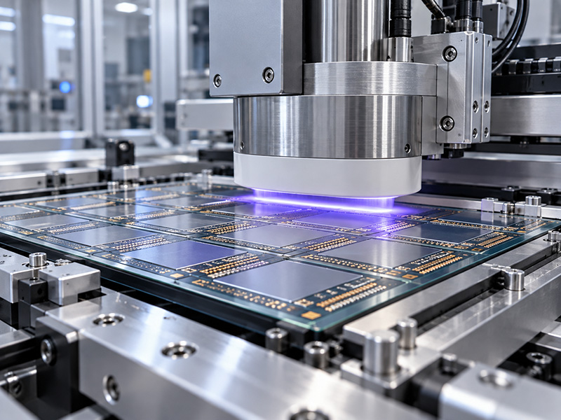
As demand for AI and high-performance computing continues to grow, semiconductor manufacturing is pursuing more than computing performance. Advanced packaging technologies—including 2.5D packaging, 3D ICs and high-density substrates—must also manage an increasing number of materials, layers and bonding interfaces.
Even when these surfaces appear clean to the naked eye, they may still contain trace organic residues, adsorbed moisture, oxides or particles. These contaminants can affect the wetting, adhesion and bonding stability of subsequent materials. Determining whether a surface is truly ready for the next process has therefore become an important challenge in high-volume advanced packaging.
Why Is Surface Cleaning Important in Advanced Packaging?
In a press release issued on October 6, 2026, E&R Engineering Corp. introduced integrated laser and plasma solutions for AI and high-performance computing packaging applications. In addition to precision laser drilling and cutting, the platform incorporates high-stability plasma systems for surface cleaning and activation, with a stated process capability index of Cpk > 1.33.
In high-density packaging, chips, substrates, adhesives, underfill materials and other functional layers must form reliable bonds. If contaminants remain on the surface or the surface energy is insufficient, materials may not wet or spread uniformly, increasing the risk of voids, uneven bonding or localized delamination.
As package dimensions become finer and the number of interfaces increases, differences in surface condition can have an even greater impact.
Plasma Cleaning Does More Than “Wash” a Surface
Plasma treatment uses energy to generate reactive species in a gas. These species interact with contaminants or molecular structures on the material surface. Depending on the gas, power, treatment time and substrate conditions, plasma treatment generally performs two main functions:
-
Surface cleaning: Helps decompose or remove trace organic residues.
-
Surface activation: Modifies surface functional groups and surface energy to improve the wetting and adhesion of adhesives, coatings or other materials.
The value of plasma treatment therefore extends beyond cleaning. It also helps establish more stable interface conditions for the next manufacturing step.
However, longer treatment times or higher power do not necessarily produce better results. If the process parameters are not compatible with the material, excessive surface modification, substrate damage or rapid degradation of the treatment effect may occur. The process must therefore be configured according to the substrate, contamination source and subsequent bonding requirements.
What Does Cpk > 1.33 Mean?
Cpk is a process capability index used to evaluate the relationship between the process mean, process variation and specification limits. A higher Cpk value generally indicates that process results are more consistently maintained within the defined specification range.
What Must Be Confirmed Before Moving from R&D to Mass Production?
Before plasma cleaning and activation can be introduced into a production line, the following factors should generally be evaluated:
-
Contamination source: Identify whether the surface contains organic residues, particles, oil or other contaminants.
-
Material compatibility: Confirm that the plasma will not damage chips, polymers, metals or functional films.
-
Treatment uniformity: Ensure consistent results across large substrates, edges and complex structures.
-
Effective time window: Some activated materials gradually return to their original surface condition, so the interval before the next process must be controlled.
-
Measurement and monitoring: Contact angle, surface energy, adhesion and reliability testing can be used to monitor process changes.
This explains why advanced packaging cannot be evaluated solely by whether a system can complete a single treatment cycle. Production speed, result consistency, process windows and quality traceability must also be considered.
Original Source
Creating Nano Technologies, Inc.
59 Alley 21 Lane 279, Chung Cheng Road, Yung Kang City, Tainan, TAIWAN
TEL:886-6-2323927 FAX:886-6-2013306 URL: http://www.creating-nanotech.com