
LP Treatment Series
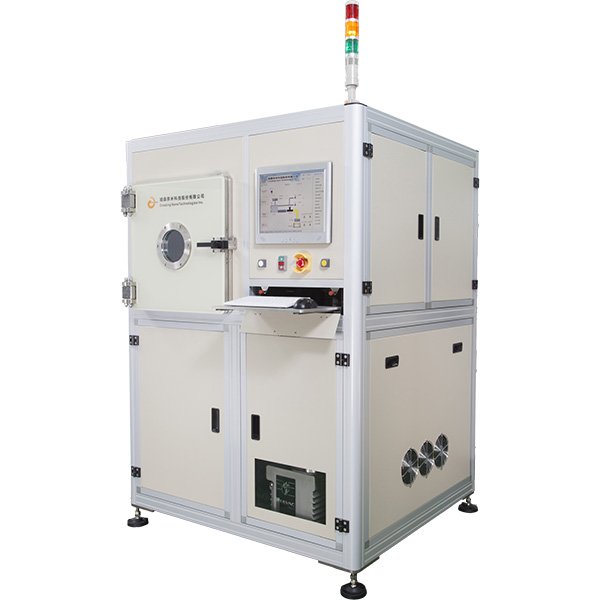
Plasma Asher PA01/PA03B
Production Description
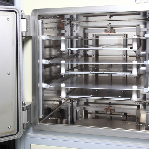
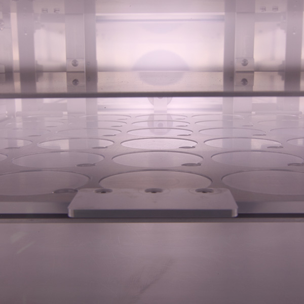
Creating Nano PC01/PA03B low pressure plasma cleaner system can be used for the fast removal of residual photo resist on wafers and clean the wafer surface with etch rates that are the highest in the industry.
Product Features
- Extremely high plasma uniformity
- No substrate damage due to the use of low energy ions
- No contamination of substrates or electrodes
- Special plasma electrode design
- High density plasma source
- High efficiency plasma
- Combined chemical reactions and physical bombardments
- Well-controlled low ion energy
- High cleaning efficiency
- Ample operating conditions
- Multiple processing gases selectivity for surface cleaning and treatment
- Fully automatic and user-friendly
- High reliability and easy maintenance
- Customization
Related solutions
- Surface cleaning and modification for LCD, IC Packaging (Flip Chip, CSP, BGA, Lead Frame, etc.), LED Packaging, SMT, PCB, FPC, etc.
- Improving surface roughness before printing, painting, gluing or bonding