
The top three semiconductor companies are attacking panel-level packaging, triggering a new battle for orders
TechNews Technology News
June 19, 2025
Author Economic Daily Li Mengshan, Yin Huizhong
June 19, 2025
Author Economic Daily Li Mengshan, Yin Huizhong
Fan-out panel-level packaging (FOPLP) is known as the next generation of advanced packaging. The three semiconductor giants, including TSMC, the leading wafer foundry, ASE, the leading semiconductor packaging and testing, and Powertech, the leading memory packaging and testing, are actively positioning themselves to grab the huge high-speed computing chip high-integration advanced packaging business opportunities of large manufacturers such as Nvidia and AMD.
The three semiconductor giants are making great advances in the field of fan-out panel-level packaging, each with its own plans, triggering a new wave of orders.
TSMC's technology is called CoPoS (Chip-on-Panel-on-Substrate), and its production capacity is located in Chiayi, and an experimental line will be set up in 2026. ASE already has a mass production 300×300mm panel-level packaging production line in Kaohsiung; Powertech has been working the longest, and achieved mass production as early as 2019, named PiFO (Pillar integration FO).
Industry analysis shows that high-speed computing chips have their own advantages in terms of high integration. Compared with wafers, panel-level fan-out packaging has a larger substrate area and can be heterogeneously integrated. It integrates circuit design with 5G communication filtering functions. After packaging, the performance and function of the chip are greatly improved, which is more suitable for various products such as 5G communications and IoT devices, and helps to further reduce the size of various consumer electronic products.
TSMC CoPoS mainly focuses on AI and high-speed computing (HPC) applications, and is rumored to be mass-produced in 2028. It is the "panelization" of CoWoS that is converted into a square design, which is conducive to the expansion of chip production capacity. TSMC's North American Technology Forum presented the latest A14 process and also announced the mass production of 9.5 times the mask size CoWoS in 2027, which can integrate more logic and memory chips into one package. The industry estimates that the trend is consistent with the development of CoPoS.
ASE already has a mass-produced 300×300mm panel-level packaging production line using the FanOut process.
Powertech named its fan-out panel-level packaging technology PiFO, which is similar to TSMC's CoPoS.
Related links: https://technews.tw/2025/06/19/foplp-big3/
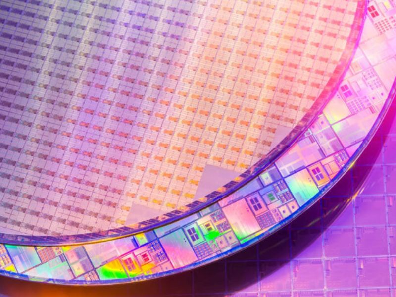
Image source: shutterstock
Image source: shutterstock
【Disclaimer】
The content of this article only represents the author's personal views and has nothing to do with Creating.
The content, text description and originality have not been verified by this site. This site does not make any guarantee or commitment to this article and all or part of the content, authenticity, completeness, and timeliness. It is for readers' reference only. Please verify the relevant content yourself.
Creating Nano Technologies, Inc.
59 Alley 21 Lane 279, Chung Cheng Road, Yung Kang City, Tainan, TAIWAN
TEL:886-6-2323927 FAX:886-6-2013306 URL: http://www.creating-nanotech.com
59 Alley 21 Lane 279, Chung Cheng Road, Yung Kang City, Tainan, TAIWAN
TEL:886-6-2323927 FAX:886-6-2013306 URL: http://www.creating-nanotech.com