

AI Chips Shift to 510 mm Large-Panel Packaging: Why Does Surface Uniformity Matter More as Panel Size Increases?
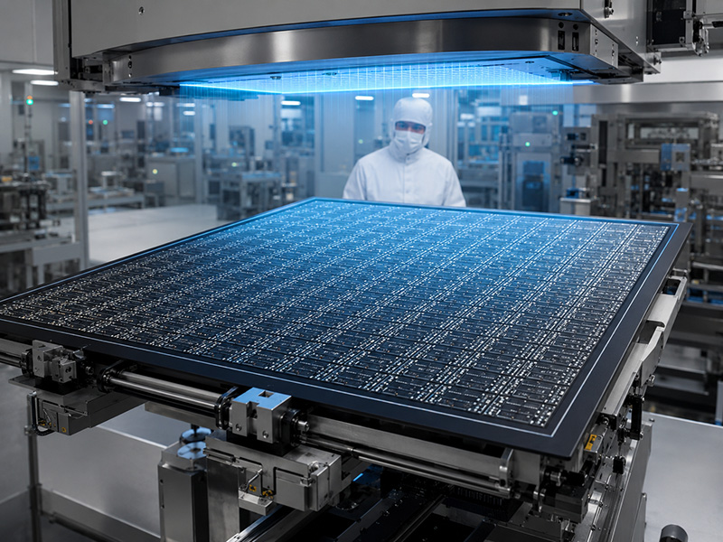
As AI chips grow larger and packaging becomes increasingly complex, the semiconductor industry is accelerating the adoption of fan-out panel-level packaging (FOPLP). Larger rectangular panels can improve manufacturing throughput and potentially reduce production costs.
Powertech Technology recently announced plans to invest approximately NT$70 billion in expanding its FOPLP capacity using 510 × 510 mm panels. Monthly capacity is expected to increase from 1,000 panels in 2026 to 5,000 panels in 2028.
According to the company, a single panel can accommodate approximately 45 AI chips, compared with eight to nine chips using wafer-level packaging, resulting in at least four times greater throughput. See the Taipei Times report
Larger Panels Magnify Process Variations
When packaging moves from circular wafers to 510 mm square panels, manufacturing equipment must maintain consistent cleanliness, temperature, flatness, and process uniformity across a much larger area.
Warpage, height variations, adhesive residue, or inconsistent surface energy across different areas of the panel may affect pattern alignment, redistribution layers (RDLs), dispensing, underfill, and bonding quality.
Nordson notes that large-format panel processing introduces challenges involving warpage control, thermal management, and dispensing accuracy. These challenges require precise height sensing, temperature control, and uniform surface preparation. See Nordson’s official information
EV Group also points out that panel warpage and die shift during packaging can cause pattern misalignment and may even affect the electrical performance of redistribution layers. Panel-level packaging therefore requires more than simply increasing the substrate size—it must deliver consistent process results at every position across the panel. See EV Group’s technical information
How Can Plasma Treatment Help Maintain Interface Quality?
Plasma cleaning and surface activation can remove trace organic contamination, adhesive residue, and surface deposits while modifying the material’s surface condition to support subsequent coating, dispensing, and bonding processes.
For large-format panels, it is not enough to confirm that treatment has been performed. Manufacturers must also evaluate treatment uniformity across the entire panel, including:
- Surface cleanliness and contact-angle distribution
- Etching or cleaning rates across different areas
- Surface roughness and thin-film uniformity
- Panel warpage and height variations
- Adhesion and reliability of subsequent materials
Creating Nano Technologies Inc. provides plasma cleaning, surface modification, thin-film processing, and customized production-line integration. Process solutions can be evaluated according to panel size, substrate material, contamination type, and downstream packaging requirements.
Panel-level packaging can significantly increase production capacity, but it also means that small surface variations may affect more chips at the same time. As packaging formats continue to expand, achieving consistent results across the entire panel will be critical to improving both manufacturing efficiency and production yield.
Sources
- Taipei Times: Powertech Books Out Panel-Level Packaging Capacity to 2030
- TrendForce: Powertech Bets NT$70B on Panel-Level AI Chip Packaging
- Nordson: Vantage XL for Panel-Level Packaging
- EV Group: Digital Lithography for Heterogeneous Integration
Creating Nano Technologies, Inc.
59 Alley 21 Lane 279, Chung Cheng Road, Yung Kang City, Tainan, TAIWAN
TEL:886-6-2323927 FAX:886-6-2013306 URL: http://www.creating-nanotech.com