

From Tin Droplets to Plasma: Why ASML Is Pushing EUV Source Power Toward 1,000W
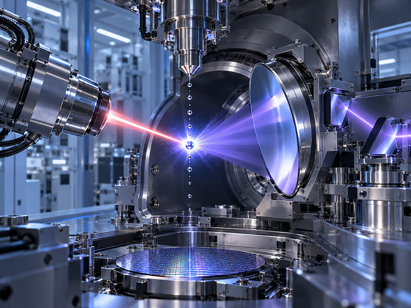
Competition in advanced semiconductor manufacturing is not limited to smaller process nodes and new chip architectures. The light-source technology behind lithography systems is also critical to production efficiency.
Modern EUV lithography systems primarily rely on laser-produced plasma technology. Powerful CO₂ laser pulses strike molten tin droplets approximately 30 micrometers in diameter, creating an ionized plasma that emits EUV radiation at a wavelength of 13.5 nanometers.
According to Tom’s Hardware, ASML has gradually increased its EUV source power from approximately 250W to around 500W. The company is now targeting 1,000W while planning to raise the tin-droplet generation rate to approximately 100,000 droplets per second.
Increasing source power is not simply about producing brighter light. Higher and more stable EUV output can improve wafer exposure speed and overall equipment productivity. However, it also creates challenges involving plasma stability, tin debris, vacuum conditions, mirror protection and precision process control.
Laser-produced plasma for EUV systems differs significantly from low-temperature plasma, atmospheric-pressure plasma and plasma-activated water. Nevertheless, these technologies share an important industrial principle: generating plasma is only the beginning. Commercial success depends on maintaining precise and repeatable control over energy, reaction conditions and process results.
From semiconductor lithography and surface modification to thin-film deposition, plasma is evolving from a specialized process tool into a foundational technology for advanced manufacturing.
Source: Tom’s Hardware
Creating Nano Technologies, Inc.
59 Alley 21 Lane 279, Chung Cheng Road, Yung Kang City, Tainan, TAIWAN
TEL:886-6-2323927 FAX:886-6-2013306 URL: http://www.creating-nanotech.com