
Creating Nano introduces SAP006 atmospheric pressure plasma cleaning equipment, leading the innovation of advanced packaging cleaning process
Economic Daily
April 15, 2025
Author: Economic Daily Zhang Jie
April 15, 2025
Author: Economic Daily Zhang Jie
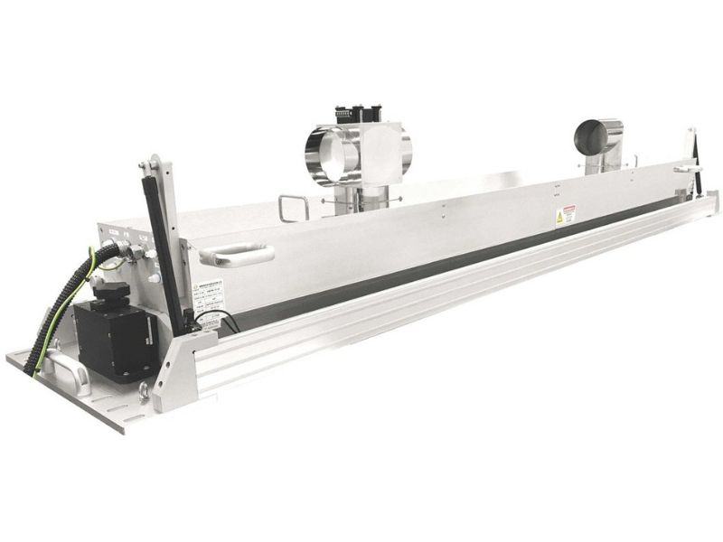
As the semiconductor industry's packaging technology is moving towards 3D, higher performance and tighter integration, Creating Nanotechnology has once again seized the industry's spotlight with its innovative technology. The atmospheric pressure plasma cleaning equipment SAP006 launched by Creating Nano not only stands out in the key links of the packaging process, but also firmly establishes its role as a key promoter in the wave of global semiconductor technology upgrades.
From smartphones, AI servers to the highly integrated chip modules of electric vehicles, chip packaging is not only a technology, but also the core of industry competitiveness. Especially as "hybrid bonding" gradually replaces traditional welding and becomes the mainstream, the cleaning process is the first line of defense to ensure the quality of the connection between chips, and its importance is greater than ever. SAP006 just fills in this puzzle piece that the market urgently needs.
The company said that the biggest advantage of SAP006 is that it can quickly remove organic pollutants on the surface of components in a normal pressure, non-vacuum environment, thereby greatly improving the stability and yield of subsequent packaging, bonding and printing. Unlike previous plasma cleaning equipment that required high temperature or vacuum conditions, SAP006 uses a patented electrode structure and high-efficiency plasma release technology to clean surfaces at high speed while maintaining uniformity, providing the best bonding foundation for various electronic components.
The device's minimized electrode design is also a highlight, which can effectively process bottom-mounted components. Whether it is touch panels, optoelectronic components or LED chip processing before packaging, it can be executed accurately without causing any damage to the metal substrate. Its modular design and simple operation interface also allow SAP006 to be easily integrated into existing automated production lines (in-line systems), providing companies with more flexible and scalable solutions.
With the booming development of emerging applications such as 5G, high-performance computing (HPC), AI and the Internet of Things, the packaging accuracy requirements for chips and substrates are becoming increasingly stringent. Especially in 2.5D/3D wafer-level packaging and fan-out packaging technology (FOPLP), how to improve the bonding yield and avoid contamination and detachment has become a daily challenge for engineers. SAP006 was born out of necessity, and can effectively solve the cleaning problems of complex materials such as ABF, LCP, PFA, etc. It not only has low-temperature characteristics (process temperature is lower than 80°C), but can also be applied to substrates with the thinnest thickness of 13μm to 200μm, combining precision and efficiency.
Overall, SAP006 is not only a cleaning device, but also a powerful tool to break through the key bottlenecks of advanced packaging production lines. As global semiconductor technology is accelerating into the next generation, Creating Nanotechnology is also proving with strength that those who truly master core technologies can not only respond to changes but also lead trends. The launch of SAP006 once again allowed the world to see Taiwan's strong strength in the field of advanced process equipment, and also provided global chip manufacturers with reliable and efficient cleaning solutions.
Related link: https://money.udn.com/money/story/5635/8676145
【Disclaimer】
The content of this article only represents the author’s personal views and has nothing to do with Creating.
The content, text and originality have not been verified by this website. This website does not make any guarantee or commitment to this article and all or part of its content, authenticity, completeness, or timeliness. It is for readers' reference only. Please verify the relevant content on your own.
Creating Nano Technologies, Inc.
59 Alley 21 Lane 279, Chung Cheng Road, Yung Kang City, Tainan, TAIWAN
TEL:886-6-2323927 FAX:886-6-2013306 URL: http://www.creating-nanotech.com